特許
登録特許13件・公開特許98件・国際特許11件
登録特許
- 河合、感光性樹脂塗布装置、特許 1614190(1984)
- 河合ほか、半導体記憶装置の製造方法、特許1875148(1985)
- 河合ほか、パターンの位置合わせずれ量評価方法、特許1650326(1985)
- 河合、密着強化剤塗布方法、特許2027790(1986)
- 河合ほか、塗布方法、特許2032170(1986)
- 河合ほか、レジスト膜形成装置、特許2613183(1986)
- 河合ほか、レジスト膜の塗布方法、特許1953374(1988)
- 河合、微細レジストパターンの形成方法、特許2565754(1988)
- 河合ほか、半導体装置の製造方法、特許 2580681(1988)
- 河合、フォトマスク、特許 2641589(1990)
- 河合ほか、現像装置、特許公報(B2) 平3-185710(1991)
- 河合、振動測定装置及び振動測定方法, 特許5004223号 (2012)
- 河合ほか、ナノ気泡の判別方法及びその装置, 特許5013320号 (2012)
公開特許
(1997年以前の出願特許は、特許戦略により審査請求をしていない。)
- 河合ほか、配線パターン形成方法、公開特許公報(A) 昭60-57622(1983)
- 河合ほか、半導体装置の製造方法、公開特許公報(A) 昭60-202954(1984)
- 河合ほか、半導体装置の製造方法、公開特許公報(A) 昭60-246630(1984)
- 河合ほか、半導体装置の製造方法、公開特許公報(A) 昭61-4247(1984)
- 河合、感光性樹脂塗布装置、公開特許公報(A) 昭61-22627(1984)
- 河合ほか、半導体記憶装置の製造方法、公開特許公報(A) 昭62-144351(1985)
- 河合ほか、半導体記憶装置、公開特許公報(A) 昭62-141758(1985)
- 河合ほか、半導体記憶装置の製造方法、公開特許公報(A) 昭62-141757(1985)
- 河合ほか、半導体記憶装置、公開特許公報(A) 昭62-141756(1985)
- 河合ほか、半導体記憶装置の製造方法、公開特許公報(A) 昭62-141759(1985)
- 河合ほか、半導体集積回路装置、公開特許公報(A) 昭62-140458(1985)
- 河合ほか、半導体装置の製造方法、公開特許公報(A) 昭62-086725(1985)
- 河合ほか、半導体製造装置、公開特許公報(A) 昭62-086724(1985)
- 河合ほか、パターン位置合わせずれ量評価方法、公開特許公報(A) 昭62-086741(1985)
- 河合、レジストパターン形成方法、公開特許公報(A) 昭62-086726(1985)
- 河合ほか、液体吐出装置、公開特許公報(A) 昭62-61668(1985)
- 河合ほか、樹脂塗布方法、公開特許公報(A) 昭62-27074(1985)
- 河合、レジストパターン形成方法、公開特許公報(A) 審判平03-003071 (1985)
- 河合、半導体記憶装置、公開特許公報(A) 昭62-202555(1986)
- 河合、密着強化剤塗布方法、公開特許公報(A) 昭62-211643(1986)
- 河合ほか、処理液塗布装置、公開特許公報(A) 昭63-136528(1986)
- 河合ほか、レジスト塗布膜厚制御装置、公開特許公報(A) 昭63-131517(1986)
- 河合ほか、半導体製造におけるフォトレジスト塗布装置、公開特許公報(A) 昭63-119531(1986)
- 河合ほか、半導体装置の製造方法、公開特許公報(A) 昭63-312643(1987)
- 河合ほか、半導体装置の製造方法、公開特許公報(A) 昭63-260079(1987)
- 河合ほか、半導体記憶装置、公開特許公報(A) 昭63-260066(1987)
- 河合、シリカガラス液吐出装置、公開特許公報(A) 昭63-278234(1987)
- 河合ほか、処理シーケンス自動設定装置、公開特許公報(A) 昭63-265303(1987)
- 河合、薬液加圧装置、公開特許公報(A) 昭63-258634(1987)
- 河合ほか、半導体装置の製造方法、公開特許公報(A) 昭63-221665(1987)
- 河合ほか、塗布装置、公開特許公報(A) 昭63-110637(1988)
- 河合ほか、スタテイック型半導体記憶装置およびその製造方法、昭63-237462 (1987)
- 河合ほか、半導体装置の製造方法、公開特許公報(A) 平1-217915(1988)
- 河合ほか、露光方法、公開特許公報(A) 平1-283926(1988)
- 河合、ウエハチャック、公開特許公報(A) 平1-283930(1988)
- 河合、半導体ウエハの現像装置、公開特許公報(A) 平1-260823(1988)
- 河合、塗布膜形成方法、公開特許公報(A) 平1-253920(1988)
- 河合、塗布膜除去装置、公開特許公報(A) 平1-253923(1988)
- 河合ほか、パターン形成方法、公開特許公報(A) 平1-123232(1987)
- 河合ほか、レジストパターン形成方法、公開特許公報(A) 平1-132123(1987)
- 河合ほか、パターンの形成方法、公開特許公報(A) 平1-134917(1987)
- 河合ほか、電極配線の形成方法、公開特許公報(A) 平1-130546(1987)
- 河合、露光方法、公開特許公報(A) 平2-010818(1988)
- 河合ほか、半導体装置の光学特性評価装置、公開特許公報(A) 平2-014544(1988)
- 河合ほか、半導体ウエハ搬送装置、公開特許公報(A) 平2-014545(1988)
- 河合ほか、パターン形成方法、公開特許公報(A) 平2-015615(1988)
- 河合ほか、パターン形成方法、公開特許公報(A) 平2-037352(1988)
- 河合、ウエハ周辺露光装置、公開特許公報(A) 平2-037712(1988)
- 河合、フォトレジストの露光方法および露光装置、公開特許公報(A)平2-063058(1988)
- 河合、パターン形成方法、公開特許公報(A) 平2-069929(1988)
- 河合ほか、レジスト膜の塗布方法、公開特許公報(A) 平2-074948(1988)
- 河合、微細レジストパターンの形成方法、公開特許公報(A) 平2-89060(1988)
- 河合、露光装置、公開特許公報(A) 平2-097011(1988)
- 河合ほか、レジスト塗布装置、公開特許公報(A) 平2-113518(1988)
- 河合、レジスト塗布装置、公開特許公報(A) 平2-129912(1988)
- 河合、露光装置、公開特許公報(A) 平2-153518(1988)
- 河合ほか、現像装置、公開特許公報(A) 平3-185710(1989)
- 河合、微細パターン形成方法、公開特許公報(A) 平3-185711(1989)
- 河合、微細パターン形成方法、公開特許公報(A) 平3-198133(1989)
- 河合、スピナー装置、公開特許公報(A) 平3-219619(1990)
- 河合、レジストパターン形成方法、公開特許公報(A) 平3-223760(1990)
- 河合、微細パターン形成方法、公開特許公報(A) 平3-235948(1990)
- 河合、微細パターン形成方法、公開特許公報(A) 平3-237458(1990)
- 河合、微細パターン形成方法、公開特許公報(A) 平3-259257(1990)
- 河合、半導体ウエハ用ステージ、公開特許公報(A) 平4-111339(1990)
- 河合、位置合わせマーク形成方法、公開特許公報(A) 平4-115517(1990)
- 河合、アライメントマークおよびその形成方法、公開特許公報(A) 平4-122012(1990)
- 河合ほか、電界効果トランジスタ、公開特許公報(A) 平4-163961(1990)
- 河合、半導体ウエハ搬送体、公開特許公報(A) 平4-271138(1990)
- 河合、半導体装置、公開特許公報(1990)
- 河合、フォトレジスト露光装置、公開特許公報(1990)
- 河合、高反射基板上でのパターニング、公開特許公報(1990)
- 河合、露光装置、公開特許公報(1990)
- 河合、フォトマスク、公開特許公報(1991)
- 河合、微細パターン形成方法、公開特許公報(1991)
- 河合、微細パターン形成方法、公開特許公報(1991)
- 河合、フォトマスク、公開特許公報(1991)
- 河合、パターン位置合わせずれ量評価方法、公開特許公報(A) 平3(1991)
- 河合、Alignment Mark having Regions Formed by Energy Beam Irradiation Therein and Method of Manufacturing the Same, 公開特許公報(A) 平3(1991)
- 河合、半導体装置の製造方法、公開特許公報(A) 特開平06-37193 (1992)
- 河合、半導体装置の製造方法、公開特許公報(A) 特開平06-89894 (1992)
- 河合、半導体装置の製造方法、公開特許公報(A) 特開平06-163453 (1992)
- 河合、半導体装置の製造方法、公開特許公報(A) 特開平06-97068 (1992)
- 河合、半導体装置の製造方法、公開特許公報(A) 特開平06-61360 (1992)
- 河合、半導体装置の製造方法、公開特許公報(1992)
- 河合、半導体装置の製造方法、公開特許公報(1992)
- 河合、露光装置、公開特許公報(1992)
- 河合、平坦化方法、公開特許公報(1993)
- 河合、半導体装置の製造方法、公開特許公報(1993)
- 河合ほか、レジストを用いた型及びその製造方法、コンタクトプローブ及びその製造方法、公開特許公報(A) 特開平11-326376 (1998)
- 河合、固体表面の微小付着物の物性評価方法、公開特許公報(A) 特開平11-248619 (1998)
- 河合ほか、基板表面の汚染度検出方法及び基板表面の汚染度検出装置、公開特許公報(A) 特開平11-248617 (1998)
- 河合、カンチレバー型の吸着センサー並びに吸着力解析方法、公開特許公報(A) 特開2000-214072 (1999)
- 河合、試料表面の付着物検査システム、試料表面の付着物検査方法、試料表面の付着物固着システム並びに試料表面の付着物処理システム、公開特許公報(A)特願平11-332081 (1999)
- 河合ほか、付着強度試験方法および装置、特許出願済み (2003)
- 河合ほか、屈折率分布の解析方法、特願2007-38310号 (2007)
- 河合、振動測定装置及び振動測定方法、特願2007-169543号 (2007)
- 河合ほか、ナノ気泡の判別方法及びその装置、特願2007-293673号(2007)
国際特許
- 河合、アメリカ , Method for Applying a Treatment Liquidon a Semiconductor Wafer, 4702796 (1987)
- 河合ほか,アメリカ , Method for Applying a Treatment Liquidon a Semiconductor Wafer, 4763182 (1988)
- 河合、韓国, Semiconductor Memory Device, 35129(1990)
- 河合、ドイツ , Verfahren zur Herstellung einer Halbleiterspei-chereinrichtung, 3639375(1990)
- 河合、ドイツ Verfahren zur Herstellung einer Halbleiterspei-chereinrichtung, 3639375 (1990)
- 河合、イギリス, Semiconductor Memory Device, 0227381(1991)
- 河合、フランス , Semiconductor Memory Device, 0227381(1991)
- 河合、アメリカ , Method for Applying a Treatment Liquidon a Semiconductor Wafer, 5001084 (1991)
- 河合、ドイツ , Verfahren zum Herstellen einer Halbleiterspei- chereinrichtung,3642595 (1991)
- 河合、ドイツ , Verfahren zur Herstellung einer Halbleiterspei-chereinrichtung, 3639058 (1991)
- 河合、ドイツ Verfahren zur Herstellung einer Halbleiterspei- chereinrichtung, 3681571 (1991)
著書
監修2冊・単著6冊・共著40冊
監修
高周波対応基板材料の開発動向と応用展開
- 執筆箇所
- :第1編 第1章 高周波対応基板の基礎と今後の動向(P3~12)、第3編 第17章 レジストリソグラフィー技術(P204~221)、第3編 第21章 プリント基板用の電極接合材料の最適化(P261~271)、第4編 第23章 高周波対応基板の信頼性・耐久性・寿命試験(P286~296)
- 出版
- :シーエムシー出版 2021年
- 総ページ数
- :196ページ
- ISBN
- :978-4-7813-1590-4
最新フォトレジスト材料開発とプロセス最適化技術
- 執筆箇所
- :第I編 第1章 リソグラフィープロセス概論(P1~11)、第III編 第1章 最適化のための技術概論(P105~115)、第III編 第3章 多層レジストプロセス(P124~131)、第III編 第6章 フォトレジストプロセスに起因した欠陥(P175~185)、第IV編 第4章 ナノスケール寸法計測(プローブ顕微鏡)(P241~248)、第IV編 第5章 付着凝集性解析(DPAT法)による特性評価(P249~259)、第VI編 第2章 密着強化処理(シランカップリング処理)の最適化技術(P303~312)
- 出版
- :シーエムシー出版 2017年
- 総ページ数
- :320ページ
- ISBN
- :978-4-7813-1263-7
単著
コーティング技術の基礎と実践的トラブル対応
- 出版
- :シーエムシー・リサーチ 2022年
- 総ページ数
- :196ページ
- ISBN
- :978-4-910581-21-7
レジスト材料の基礎とプロセス最適化
- 出版
- :シーエムシー・リサーチ 2021年
- 総ページ数
- :193ページ
- ISBN
- :978-4-910581-10-1
レジスト材料・プロセスの使い方ノウハウとトラブル解決
- 出版
- :R&D支援センター 2018年
- 総ページ数
- :185ページ
- ISBN
- :978-4-905507-25-3
一発必中シリーズ「欠陥を出さない!良い塗布膜を得るためのコントロール技術」
- 出版
- :サイエンス&テクノロジー 2012年
- 総ページ数
- :197ページ
- ISBN
- :978-4-86428-046-4
現場で応用できるコーティングの理論と現象 -トラブルをメカニズムから考える-
- 出版
- :加工技術研究会 2012年
- 総ページ数
- :184ページ
- ISBN
- :978-4906451449
塗膜・レジスト膜の乾燥・付着技術とトラブル対策
- 出版
- :情報機構 2011年
- 総ページ数
- :196ページ
- ISBN
- :978-4-904080-75-7
共著
シランカップリング剤の基礎と応用
- 執筆箇所
- :第2章 第10節 シランカップリング剤の評価と半導体分野への応用(p114~135)
- 出版
- :シーエムシー出版 2025年
- 総ページ数
- :249ページ
- ISBN
- :978-4-7813-1919-3
半導体製造におけるエッチング技術
- 執筆箇所
- :第2章 第1節 ウェットエッチングの基礎と不良対策(p25~50)
- 出版
- :シーエムシー出版 2025年
- 総ページ数
- :235ページ
- ISBN
- :978-4-7813-1872-1
塗工(塗布・乾燥)プロセスの基礎と実践
- 執筆箇所
- :第2章 第1節 塗布膜乾燥の基本とプロセス・現象・本質の理解&最適化と欠陥・トラブル対策(p79~90)
- 出版
- :R&D支援センター 2025年
- 総ページ数
- :392ページ
- ISBN
- :978-4-905507-80-2

塗布・乾燥のトラブル対策
- 執筆箇所
- :第2章 第6節 塗布・コーティング膜の制御と各種トラブル対策~異物、密着性、ピンホール~
- 出版
- :技術情報協会 2023年
- 総ページ数
- :563ページ
- ISBN
- :978-4-86798-131-3

先端半導体製造プロセスの最新動向と微細化技術
- 執筆箇所
- :第1節 半導体における付着、脱離メカニズム(p521~529)
- 出版
- :技術情報協会 2023年
- 総ページ数
- :639ページ
- ISBN
- :978-4-86104-982-8
導体製造におけるウェット/ドライエッチング技術
- 執筆箇所
- :第2章 第3節 ウェットエッチングの高精度化とトラブル対策(p67~94)
- 出版
- :R&D支援センター 2022年
- 総ページ数
- :252ページ
- ISBN
- :978-4-905507-61-1
フォトレジストの最先端技術
- 執筆箇所
- :第4編 第1章 実用化における最適化技術(p168~191)
- 出版
- :シーエムシー出版 2022年
- 総ページ数
- :345ページ
- ISBN
- :978-4-7813-1679-6
-5G/Beyond 5Gに向けた- 高速・高周波対応部材の最新開発動向
- 執筆箇所
- :第2章 14節 ソルダーレジストの高周波対応とプロセス(P.173~178)
- 出版
- :技術情報協会 2021年
- 総ページ数
- :653ページ
- ISBN
- :978-4-86104-828-9
接着・接合の支配要因と最適化技術
- 執筆箇所
- :第1章 13 電子材料における接着・接合技術と密着不良、界面破壊、剥離対策(P.88~93)
- 出版
- :S&T出版 2021年
- 総ページ数
- :270ページ
- ISBN
- :978-4-907002-84-8
シランカップリング剤の最新技術動向
- 執筆箇所
- :第5章 第1節 シランカップリング剤による濡れ性・付着制御(p70~86)
- 出版
- :シーエムシー出版 2020年
- 総ページ数
- :231ページ
- ISBN
- :978-4-7813-1520-1
クリーンルームの微小異物・汚染物対策と作業員教育
- 執筆箇所
- :第7章 第4節 半導体表面への粒子付着のメカニズムと測定・防止(P.260~266)
- 出版
- :技術情報協会 2020年
- 総ページ数
- :523ページ
- ISBN
- :978-4-86104-805-0
プリント配線板材料の開発と実装技術
- 執筆箇所
- :第12章 第2節 レジストプロセスの最適化とトラブル対策(P.542~554)
- 出版
- :技術情報協会 2020年
- 総ページ数
- :713ページ
- ISBN
- :978-4-86104-787-9
高分子の残留応力対策
- 執筆箇所
- :第8章 第3節 塗膜の内部応力による欠陥現象とその対策(P403~420)
- 出版
- :技術情報協会 2017年
- 総ページ数
- :480ページ
- ISBN
- :978-4-86104-648-3
シランカップリング剤の使いこなし ノウハウ集
- 執筆箇所
- :第8章 第7節 レジストにおけるシランカップリング剤処理装置の構成,最適化と剥離トラブル対策(P304~316)
- 出版
- :技術情報協会 2016年
- 総ページ数
- :384ページ
- ISBN
- :978-4-86104-610-0
最新高機能コーティングの技術・材料・評価
- 執筆箇所
- :第4編 第2章 コーティング膜の凝集コントロールと評価(P194~206)
- 出版
- :シーエムシー出版 2015年
- 総ページ数
- :233ページ
- ISBN
- :978-4-7813-1098-5
高分子における劣化・破壊現象の写真・データ事例集
- 執筆箇所
- :第14章 第6節 塗膜の乾燥不良事例 ~クラック、密着不良~(P449~516)
- 出版
- :技術情報協会 2014年
- 総ページ数
- :729ページ
- ISBN
- :978-4-86104-496-0
気泡・ボイドの発生メカニズムと未然防止・除去技術
- 執筆箇所
- :第1章 第2節 塗るときなぜ気泡が発生するのか?(P7~17)
- 出版
- :技術情報協 2014年
- 総ページ数
- :554ページ
- ISBN
- :978-4-86104-502-8
薄膜塗布技術と乾燥トラブル対策
- 執筆箇所
- :第8章 第8節 超臨界乾燥(P528~533)、第10章 第6節 レべリング性と乾燥速度の両立(P641~647)、第10章 第11節 さらに高品位な膜を作るためのテクニック(P670~676)
- 出版
- :技術情報協会 2013年
- 総ページ数
- :825ページ
- ISBN
- :978-4-86104-490-8
シランカップリング剤の効果と使用法
- 執筆箇所
- :第7章 第6節 レジストにおけるシランカップリング剤の効果と使用方法および処理装置(P256~258)
- 出版
- :S&T出版 2012年
- 総ページ数
- :395ページ
- ISBN
- :978-4-907002-07-7
粒子分散系塗布膜を中心にした高粘度スラリーの調液・塗布・乾燥技術
- 執筆箇所
- :第2章 第1節 乾燥膜におけるトラブルを防ぐために抑えておく乾燥理論(P79~89)、第2章 第5節 各種乾燥プロセスにおける装置選定技術(P134~144)、第2章
第6節 乾燥プロセスにおけるトラブル原因・対策(P145~161)
- 出版
- :技術情報協会 2011年
- 総ページ数
- :336ページ
- ISBN
- :978-4-86104-363-5
バインダー(結着剤)の失敗しない選び方・使い方事例集
- 執筆箇所
- :第6節 乾燥時のバインダー使用の留意点と条件設定、第7節 バインダー乾燥・焼成装置の機構と条件設定、第8節 バインダー乾燥・焼成後のトラブル事例および対策(P149~182)
- 出版
- :技術情報協会 2011年
- 総ページ数
- :262ページ
- ISBN
- :978-4-86104-381-9
レジストプロセスの最適化テクニック ~微細化・トラブル解消のための工程別対策および材料技術~
- 執筆箇所
- :第8章第1節第4-8項 (P294~333)、第2節第1項 (P334~P351)
- 出版
- :情報機構 2011年
- 総ページ数
- :557ページ
- ISBN
- :978-4-904080-90-0
挑戦こそが成功の鍵
- 執筆箇所
- :第1章 なぜコンピュータは速くなり続けるのか?(P51~56)
- 出版
- :近代科学社 2010年
- 総ページ数
- :263ページ
- ISBN
- :978-4-764950-21-4
コーティング材料のコントロールと添加剤の活用
- 執筆箇所
- :第2章 第6節 電子材料のコーティングにおける添加剤の活用(P84~101)
- 出版
- :サイエンス&テクノロジー 2010年
- 総ページ数
- :329ページ
- ISBN
- :978-4-903413-82-2
剥離対策と接着・密着性の向上
- 執筆箇所
- :第3節 レジスト膜における付着・剥離コントロール(P267~289)
- 出版
- :サイエンス&テクノロジー 2010年
- 総ページ数
- :436ページ
- ISBN
- :978-4-903413-89-1
シランカップリング剤の反応メカニズムと処理条件の最適化
- 執筆箇所
- :第4章 シランカップリング処理における処理装置構成と処理プロセスの最適化(P67~76)
- 出版
- :技術情報協会 2010年
- 総ページ数
- :321ページ
- ISBN
- :978-4-86104-307-9
インクジェット技術における微小液滴の吐出・衝突・乾燥
- 執筆箇所
- :第3章 第2節 [1] 固体表面のシランカップリング剤処理とぬれ性評価(P376~388)
- 出版
- :技術情報協会 2009年
- 総ページ数
- :415ページ
- ISBN
- :978-4-86104-291-1
プリンタブル・エレクトロニクス 技術開発 最前線 ~材料開発・応用技術編~
- 執筆箇所
- :第1章 第3節 微小液滴の基礎物性とその制御(P21~30)
- 出版
- :技術情報協会 2008年
- 総ページ数
- :294ページ
- ISBN
- :978-4-86104-209-6
薄膜の機械的物性と不良対策・高品質化
- 執筆箇所
- :第4章 第14節 フォトレジスト薄膜の特性と不良対策(P254~271)
- 出版
- :サイエンス&テクノロジー 2008年
- 総ページ数
- :328ページ
- ISBN
- :978-4-903413-42-6
接着強度試験法および接着界面の解析・評価事例
- 執筆箇所
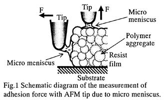
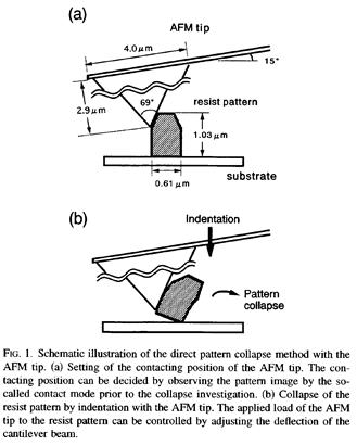
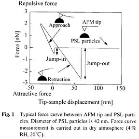
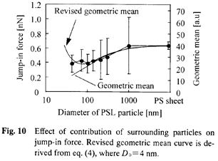
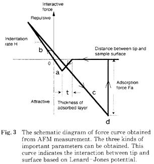
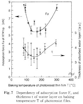
- :第2章 第1節 原子間力顕微鏡(AFM)を用いた接着層解析(P49~71)
- 出版
- :情報機構 2007年
- 総ページ数
- :242ページ
- ISBN
- :978-4-901677-93-6
泡コントロールと消泡・脱泡事例集
- 執筆箇所
- :第17節 レジストパターン上の気泡除去(P242~250)
- 出版
- :技術情報協会 2007年
- 総ページ数
- :260ページ
- ISBN
- :978-4-86104-188-4
インクジェットプリンターの応用と材料Ⅱ
- 執筆箇所
- :第2章 インクジェットインク・微小液滴の基礎物性(P12~23)
- 出版
- :シーエムシー出版 2007年
- 総ページ数
- :277ページ
- ISBN
- :978-4-88231-966-5

表面・深さ方向の分析方法
- 執筆箇所
- :第3章 第14節 レジスト(P365~378)
- 出版
- :サイエンス&テクノロジー 2007年
- 総ページ数
- :618ページ
- ISBN
- :978-4-903413-30-3
新しい分散・乳化の科学と応用技術の新展開
- 執筆箇所
- :第3章 第9節 2.接着界面でのミクロな粘性指状変形と接着性(P572~583)
- 出版
- :テクノシステム 2006年
- 総ページ数
- :1003ページ
- ISBN
- :978-4-924728-50-0
乾燥大全集
- 執筆箇所
- :第13章 第3節 レジストの乾燥過程の解析(P363~380)
- 出版
- :情報機構 2006年
- 総ページ数
- :522ページ
- ISBN
- :978-4-901677-60-8
半導体・液晶ディスプレイ フォトリソグラフィ技術ハンドブック
- 執筆箇所
- :第2編 第1章 第2節 下地基板とレジストとの親和性(P35~40)
- 出版
- :リアライズ社 2006年
- 総ページ数
- :587ページ
- ISBN
- :978-4-89808-069-3
接着剤の設計と接着製品の信頼性を重視した粘着技術の3A
- 執筆箇所
- :第2章 3.AFMによる接着挙動の解析(P82~90)
- 出版
- :リアライズAT 2006年
- 総ページ数
- :347ページ
- ISBN
- :978-4-89808-077-4
最新レジスト材料ハンドブック
- 執筆箇所
- :第6節 レジスト膜の機械的性質の分析.評価(P208~222)
- 出版
- :情報機構 2005年
- 総ページ数
- :315ページ
- ISBN
- :978-4-901677-45-4
表面・界面工学大系(下巻)応用編
- 執筆箇所
- :第8章 第5節 接着研究の最先端(P160~173)
- 出版
- :テクノシステム 2005年
- 総ページ数
- :1393ページ
- ISBN
- :978-4-924728-49-7
超LSI技術14 デバイスとプロセス その4
- 執筆箇所
- :9.高解像フォトレジストプロセス(P275~311)
- 出版
- :工業調査会発行 1990年
- 総ページ数
- :354ページ
- ISBN
- :978-4-7693-1083-8
TV取材・新聞発表
6件
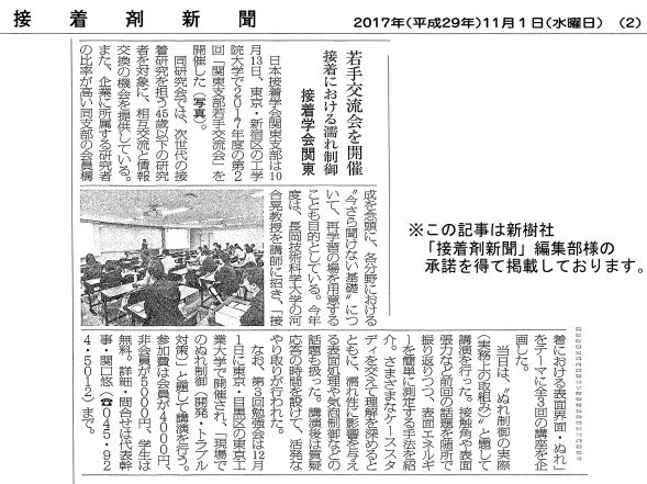
接着剤新聞 掲載
掲載日:H29.11.1
接着剤新聞に、弊社代表取締役社長 河合が講師を務めた講座ついて掲載されました。
H29.10.13に日本接着学会関東支部が、東京工業大学で開催した第2回若手交流会「接着における表面界面・ぬれ」勉強会にて、"ぬれ制御の実際(実務上の取組み)"と題して講演を行いました。
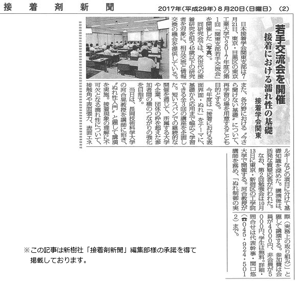
接着剤新聞 掲載
掲載日:H29.8.20
接着剤新聞に、代表取締役社長 河合が講師を務めた講座ついて掲載されました。
H29.7.21に日本接着学会関東支部が、東京工業大学で開催した第1回若手交流会「接着における表面界面・ぬれ」勉強会にて、"ぬれ性入門"と題して講演を行いました。
長岡ケーブルテレビ(テクノ探検隊)
取材日:H25.2.2
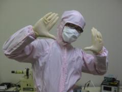
テクノ探険隊は、長岡技術科学大学とエヌ・シィ・ティ(旧 長岡ケーブルテレビ)との共同企画番組です。長岡技術科学大学の最先端技術に隠された謎を解くために結成されたテクノ探検隊の小学生たちが長岡技術科学大学に潜入する内容です。
河合研究室では、長岡地域の小学生を対象に、大学内のクリーンルームについて探検し、様々な発見を通して科学へ親しんでもらうことを目的に番組を作製しました。
平成25年3月12日に放映されました。
(キャッチフレーズ)
「そうじ」しなくてもいい教室が、大学にあるよ。
いつもは気づかない身近なミクロの世界
見て!触れて!作って!発見しよう!
テレビ取材(SOS危機一髪)
取材日:H15.4.18
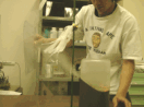
フジテレビのTV番組(SOS危機一髪)に、帯電した衣服の除電法について取材協力しました。
衣服・下敷き等を摩擦により帯電させ、水蒸気(息)を当て除電しました。
最終的に放映はされませんでしたが、意外な方法で除電できることを示しました。
NHK取材(科学大好き土曜塾)
取材日:H14.5.28
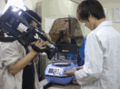
NHKの教育番組(科学大好き土曜塾)に対し、接着剤の接着メカニズムについて取材協力しました。
木材・プラスチックなどを接着させ、その接着面の観察を行い、接着剤と各種試料の関係(アンカー効果)からそれぞれの接着性を示しました。
平成14年6月8日に放映されました。
NHK取材(ためしてガッテン)
取材日:H14.4.2
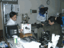
NHKの一般番組(ためしてガッテン)の取材があり、接着剤の接着メカニズムで重要である表面解析について撮影しました。
河合研究室の接触角計を用いて、物質表面の洗浄度や汚染度について示しました。
平成14年5月15日に放映されました。